Magnetocapacitance effect
Magnetocapacitance (MC) effect has attracted much attention due to their fascinating spin phenomena, such as spin capacitance, frequency-dependent spin transport and potential applications as highly-sensitive magnetic sensors, high-frequency devices and energy storage materials. The MC effect has been observed in multiferroic materials, spintronic devices and magnetic supercapacitors. Here, the spintronic devices include magnetic tunnel junctions (MTJs), molecular spin valves, magnetic nanogranular films and magnetic single-electron transistors (SETs).
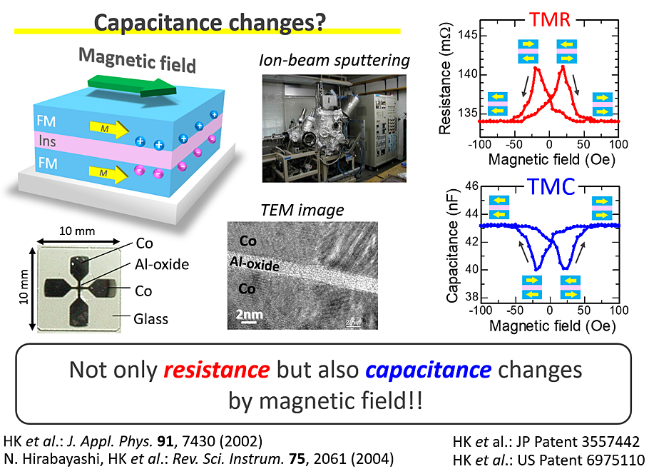
MTJs consist of two ferromagnetic layers separated by a thin insulator. MTJs show a large tunnel magnetoresistance (TMR) effect at room temperature. At present, the TMR ratio has reached up to 600% in MTJs with MgO tunnel barriers. On the other hand, MTJs exhibit tunnel magnetocapacitance (TMC) effect at room temperature (JAP, 2002). In TMC effect, when the spins in both magnetic electrodes are parallel to each other, to be referred to as the parallel (P) configuration, the capacitance CP is larger than CAP in the antiparallel (AP) configuration.
A few years ago, we have observed a large TMC beyond 150% (APL, 2015), which is three times larger than the conventional value, at room temperature in MTJs with MgO tunnel barriers. We have also found that the mechanism of TMC can be well explained by the theoretical calculation based on Debye-Fröhlich (DF) model.
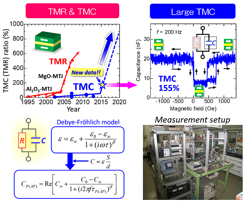
According to the model, we can predict an inverse TMC, in which CAP is larger than CP, using magnetic materials showing negative spin polarization. In fact, we have successfully observed the inverse TMC for the first time in Fe/AlOx/Fe3O4 MTJs (Scientific Reports, 2017). More recently, we have observed a new phenomenon of a voltage-induced TMC, in which TMC increases with biasing voltage in an MTJ system based on Co40Fe40B20/MgO/Co40Fe40B20 (Scientific Reports, 2018). The extended DF model predicts that the voltage-induced TMC ratio could reach 1100% in MTJs with a corresponding TMR value of 604%. Our work has provided a new understanding on AC spin-dependent transport in MTJs and may open a novel pathway for spintronics applications, e.g., magnetic sensors, non-volatile memories and spin logic circuits.
Nanoscale junction utilizing magnetic thin-film edges
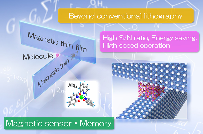
In a nanoscale junction of metal, magnetic body, and molecules, curious diverse phenomena are observed. These include the quantization of conductance by ballistic conduction, emergence of an electrical switching effect, and the generation of giant magnetoresistance effect, among others. As a way to fabricate such a nanoscale junction, various methods such as lithography, breakjunction and nanoindentation have been proposed.
Under such an environment, this laboratory has recently proposed a new fabrication method of nano-scale junction using edges of magnetic thin films (Nanotechnology, 2010; JAP 2015; Applied Surface Science 2016; JP Patent 5773491; US Patent 8795856). In this method, as edges of two magnetic thin films meet at right angles to each other, the junction area (S = d x d, where d is the film thickness) is determined by the thickness of the magnetic thin film. Accordingly, when the film thickness is from 1 to 20 nm, the junction area is from 1x1 to 20x20 nm2. Thus, ultrafine nano-scale junctions can be fabricated. This device has the potential to find further new phenomena, and thereby an attempt will be made to create a next-generation magnetoresistance or switching device and a beyond-CMOS device.
Control of surface structure and magnetic transition by light illumination
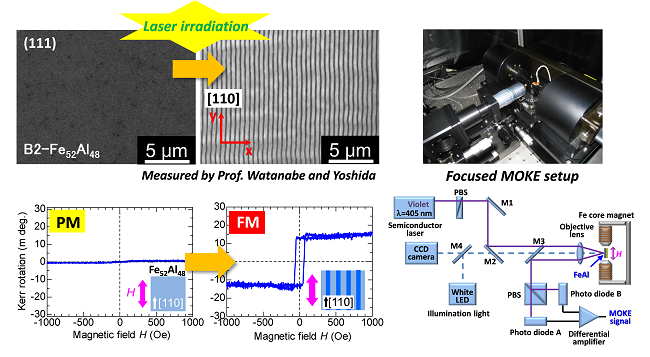
Regarding magnetic nanostructures comprised of magnetic body such as nanodot, nanostripe, nanowire and nanotube, interesting phenomena including coercivity enhancement and current-driven domain wall have been expressed. Various methods to fabricate such magnetic nanostructures such as lithography, shadow mask and ion irradiation are proposed.
Under such circumstances, the laboratory has recently revealed that nano-second irradiation of pulse laser to FeAl alloy creates change in the surface morphology and brings about paramagnet-ferromagnet magnetism transition. (joint research with Watanabe Laboratory of Hokkaido University and Yoshimi Laboratory of Tohoku University; APL 2013; JAP 2014, 2015) In terms of surface morphology, interesting structures such as nanostripe structures, nanonetwork structures and nanodot patterns can be obtained. Subsequently with this structural phase transition, the magnetism property changes from paramagnetism to ferromagnetism. These results imply potential to control not only surface and internal structures, but also magnetism through light irradiation. At present, using the same irradiation method, the laboratory is propelling an unprecedented exploratory research on nanostructured magnetic material. Moreover, in this system, the spin transport is also studied to pioneer this research field of interdisciplinary new frontier.